
In-Process Wafer Step Height Measurement
Autres thèmes interessants

L'intelligence artificielle au Laser World of Photonics : AI prompts boosts of innovation in photonics
L'intelligence artificielle est un moteur de l'innovation en photonique. Que ce soit dans la production industrielle, l'assurance qualité, la médecine…
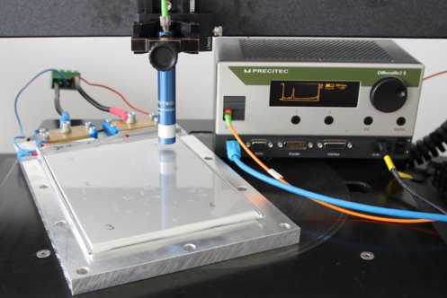
Precitec fait partie du projet de recherche Quaze
L'Institut Fraunhofer pour les systèmes énergétiques solaires ISE et Precitec travaillent ensemble dans le cadre du projet de recherche "Quaze" au…

La nouvelle boutique en ligne est en ligne !
Nous avons le plaisir de vous présenter notre toute nouvelle boutique en ligne, optimisée pour faciliter et rendre plus efficace la commande de pièces…

Signe de solidarité et de communauté
Nous sommes heureux de soutenir à nouveau cette année l'Hospice pour enfants de Karlsruhe par un don de Noël. Il accomplit un travail précieux en…
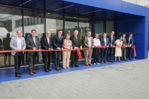
Inauguration de nos nouveaux bâtiments lors de notre fête d´été
Encore une avancée : depuis quelques semaines, nous sommes en mesure de travailler dans nos nouveaux locaux aux équipements modernes. Cet ajout de…

Cérémonie de remise du Prix de l'Innovation
Les finalistes de l'Innovation Award Laser Technology 2024 ont été officiellement présentés lors d´une cérémonie dans le cadre de la conférence AKL24…

Enovasense honored as inVision Top Innovation 2024
Thickness measurement of opaque and semi-transparent coatings with laser photothermal technology.

Pour une bonne cause
Pour l'année 2024, nous avons à nouveau décidé de soutenir différentes institutions et organisations d'utilité publique de notre région. Nous sommes…
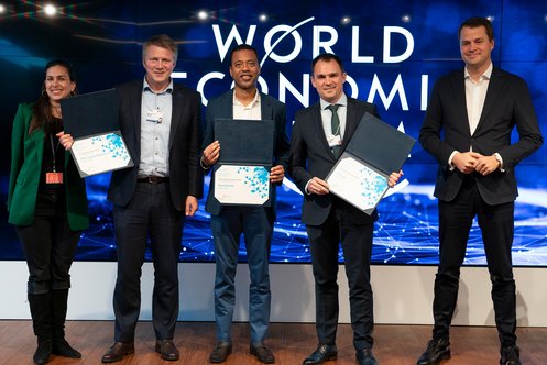
Prix pour Precitec dans la catégorie "Innovation"
L'award dans la catégorie « Innovation » du Forum économique mondial a été un véritable honneur pour Precitec. Cette reconnaissance valide tous nos…

Création de Precitec India
C'est avec impatience que tous les futurs collaborateurs de la nouvelle société Precitec India Pvt Ltd se sont réunis pour une cérémonie…