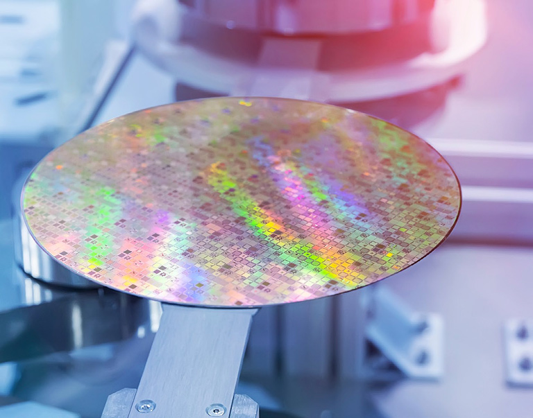
Inline quality control of wafers in the semiconductor industry
CHRocodile sensors for wafer metrology
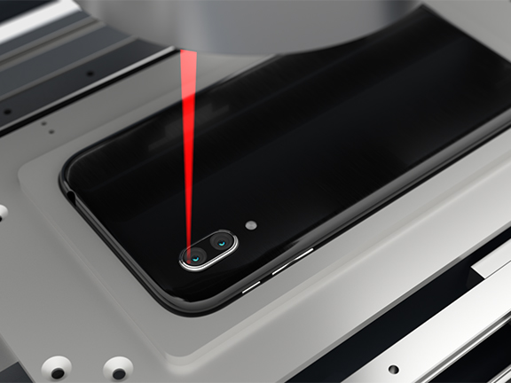
Semiconductor and microelectronic inspection sensors need to measure the gauge of wafers, determine structures in screen manufacturing, and check bonding during inline quality controls. Moreover, they also have to measure transparent coatings, and monitor mechanical and chemical removal processes in real time for quality control purposes.
With their lateral resolution in the micrometer range and high resolution in the sub-micrometer range, our CHRocodile sensors fulfill all these requirements and deliver reliable measurements in both harsh industrial and clean room environments.
Enovasense sensors, which complement Precitec's sensor portfolio, use laser photothermal technology to measure the thickness of opaque and semitransparent coatings.
Measuring opaque layer thickness
Processing wafers in the semiconductor industry involves a wide variety of coatings and layers, e.g. hard-mask layers, metallization layers, backpack layers, core semiconductor and dielectric layers. Optical or radiative technologies have their limitations in measuring opaque layers.
Laser photothermal technology from Enovasense, in contrast, enables non-contact, non-destructive, non-intrusive, non-radiative, fast and repeatable measurements of a wide range of opaque coating thicknesses. Enovasense PS offers precise non-destructive measurements of thickness of coating material through easy-to-integrate ultra-compact probes.
Detailed information on Enovasense applications for Semiconductor industry can be downloaded by filling out the form.
In-process thickness monitoring during wafer thinning and structuring
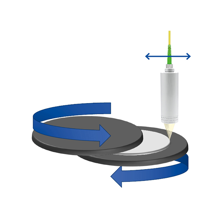
As the demand for wafers with ever-lower total thickness variation (TTV) or defined structured surface is increasing, extremely accurate in-process thickness monitoring through non-contact, non-destructive measurement technology is becoming indispensable.
The challenges come from varying wafer thickness ranges, differing prime wafer materials, and the harsh inline process environment (e.g. no clear view of the wafer because of grinding sludge). Our CHRocodile 2 IT, IT DW series and 2 DPS sensors can reliably measure greatly varying wafer thicknesses and materials (Si doped, highly doped, SIC, GaN, InP, plastics, sapphire, LiTaO) and wafer processing states.
The water- and acid-resistant probes and water jet probes are unaffected by wear and tear and thus reduce operating costs. They are also suitable for customized integration into different process machines.
Precise monitoring and control of wafer thickness by optical measuring is described in our whitepaper "CMP and grinding in the semiconductor industry". Detailed information can be downloaded by filling out the form.
Monitoring wafer bow, warp and TTV
Too large wafer bow, warp or TTV pose a great challenge for wafer handling and processing and can even cause wafer breakage and significant production losses. Measurement of these values to minimize losses has to be not only highly accurate and fast but also non-destructive, i.e. non-contact. As bow and warp change at different production steps, metrology and process feedback are crucial.
Our non-contact optical measurement technology enables in-process deployment close to the production steps where bow and warp are caused. CHRocodile 2 IT and 2 DPS sensors offer flexible solutions, with compact chromatic probes, easy refitting, and measurement of all kinds of wafers.
Inspecting dicing grooves
Monitoring dicing groove depth and width during or after material treatment safeguards the required treatment quality. Visualizing the groove also reveals any die cracks, which may lead to die breakage and expensive output losses. Measurement of the groove depth and width enables the wafer to be reworked if there is any deviation from the norm.
To image the largest possible part of the groove and identify as many die cracks as possible, fast non-contact metrology with a high lateral resolution and great accuracy is required. The CHRocodile CLS is well-suited to measuring the depth and width of dicing grooves.
If only the width needs to be measured, our Chromatic Vision Camera (CVC) is a better option because of its high speed.
Both devices have outstanding imaging quality and do not suffer from shadowing as they measure at a perpendicular angle to the sample. Moreover, height measurements are extremely accurate, lateral resolution very high, and measurements possible on steep slopes.
Measuring and inspecting solder bumps
Wafer level bumps and solder bumps are essential for electronic interconnections. Measuring their height and coplanarity safeguards interconnection quality. With bump spacing decreasing and bump density increasing, only coaxial imaging can measure topographies accurately and fast enough.
The CHRocodile CLS uses this technology for measurements of great accuracy and resolution. Moreover, coaxial imaging technology measures at a perpendicular angle to the sample and can thus measure the precise bump shape even at low spacing and on steep slopes.
Detecting of die cracks
Material treatment during dicing stresses a wafer and the silicon may crack. Visualizing dicing grooves detects such silicon cracks, which may cause die breakage during subsequent production. The thinner the wafer, the higher the risk of breakage, and the more important it is to detect these microscopic cracks.
The Chromatic Vision Camera (CVC) combines high resolution with a high depth of field to ensure sharp imaging without the need to autofocus. The line fast scanning speed of the CVC thus saves valuable time and increases throughput.
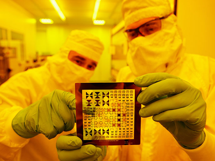
Alignment of wafer and photo mask
During photolithography µm-accurate alignment of the mask and wafer is essential. The smaller the structures, the more accurate the lateral and parallel alignment has to be. To meet these requirements, highly accurate, non-contact measurements are required.
The chromatic confocal and interferometric detectors in the CHRocodile 2 S meet these requirements and are also suitable for multiple leveling applications in the semiconductor industry. What's more, the sensors are maintenance-free and designed for non-stop operation in a production environment.
Die and wafer bonding
Die and wafer bonding is increasingly replacing traditional bonding techniques as it enables smaller bondings and IC packages, and also reduces the chip's energy consumption. However, highly accurate alignment of the dies or wafers is critical to secure IO connectivity.
Precitecs CHRocodile 2 S, CLS, 2 IT optical sensors and the Chromatic Vision Camera CVC measure the precise position, height, tilt, and rotation of the dies and enable exact wafer alignment during bonding. The great precision of chromatic confocal and interferometric sensors guarantees optimum bonding results.
Moreover, the speed of measurement allows in-process inspection which increases throughput, as does the ability to remove faulty bondings from the production process.
Inspecting probe cards
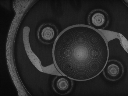
Probe cards are commonly used to conduct circuit tests on finished wafers. A probe card has numerous tiny tips that individually contact each die on the wafer and apply a test signal. The height uniformity and lateral position of the tips have to be regularly inspected to assure optimal wafer test results. With thousands of densely packed tips on each probe card, fast, coaxial and, above all, non-contact metrology is required.
The chromatic confocal technology in the CHRocodile CLS line sensor and CHRomatic Vision Camera ensures fast and reliable inspection with an extremely high degree of lateral and axial accuracy.
